Q+A with Ali Javey
Ali Javey, professor of electrical engineering and computer sciences at Berkeley since 2006, has been highly visible in the science press recently with the latest version of his “e-skin” breakthrough (see Forefront, spring 2011) and groundbreaking work on a new, low-cost method for manufacturing high-efficiency photovoltaics. Javey moved with his family from Iran to the U.S. when he was 15 and later studied at Virginia’s Old Dominion University, Stanford and Harvard. Berkeley Engineer sat down with him to find out more about his prolific research.
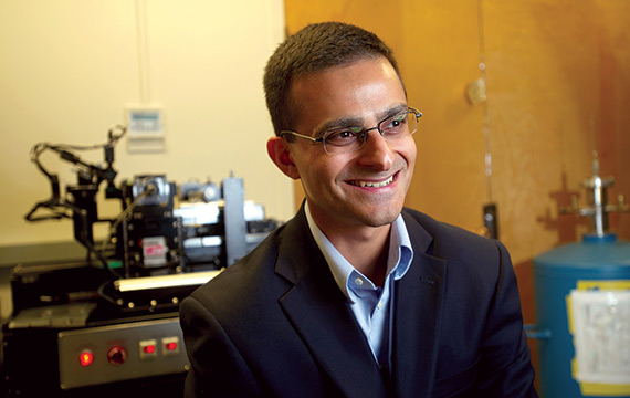
 Ali Javey (Photo by Noah Berger)What got you started in engineering?
I started studying physics, but skipped the general courses because I had taken AP physics in high school, and so I didn’t meet the degree requirements. I changed my major to biology, then again to chemistry. While working on my Ph.D., I began trying to build electronics out of carbon nanotubes, and the next thing you know I’m applying for faculty positions in chemistry, materials science and electrical engineering. I accepted the position here at EECS because it fit my interests best, exploring the use of new materials for electronics.
Where is your e-skin breakthrough headed?
Engineers see skin as the human interface to the outside world. We want to develop substrates, like human skin, that can cover different objects very uniformly and would also interface with the outside world—that’s why we call it “electronic skin.” Sensor networks in that e-skin can do 2D or even 3D mapping of different stimuli, maybe your hand motion or touch: Imagine covering the laminated dashboard of a car, or an entire wall, with networks that can, for example, sense your hand or eye movements. Future “touch” screens—you won’t touch them, you just move your hand over the screen. That’s what we’re working on now.
What’s new about the photovoltaics you are building?
Although III-V compound semiconductors have the highest efficiency, they can cost 20 times more than silicon-based semiconductors. There are two cost components: the substrate, and semiconductor growth. So we asked, first, can we use a low-cost substrate, metal foil? And second, can we come up with a completely new growth mechanism? We can now grow III-V compound semiconductors of very high quality, on metal foil, using a completely new process with very low-cost precursors.
How are these two areas of your work connected?
Both involve manipulating materials on new substrates, exotic substrates—metal foils for photovoltaics, and for e-skin, very thin plastic substrates—and coming up with new processes, fabrication technologies and device architectures. But materials innovation is the bridge.
What’s next for the Javey lab?
For those two directions that we have in our group, we’re trying to push the limits of what we can do with them. The question is: can we start to transition some of our work to industry? So that’s going to be our goal for the next few years.

