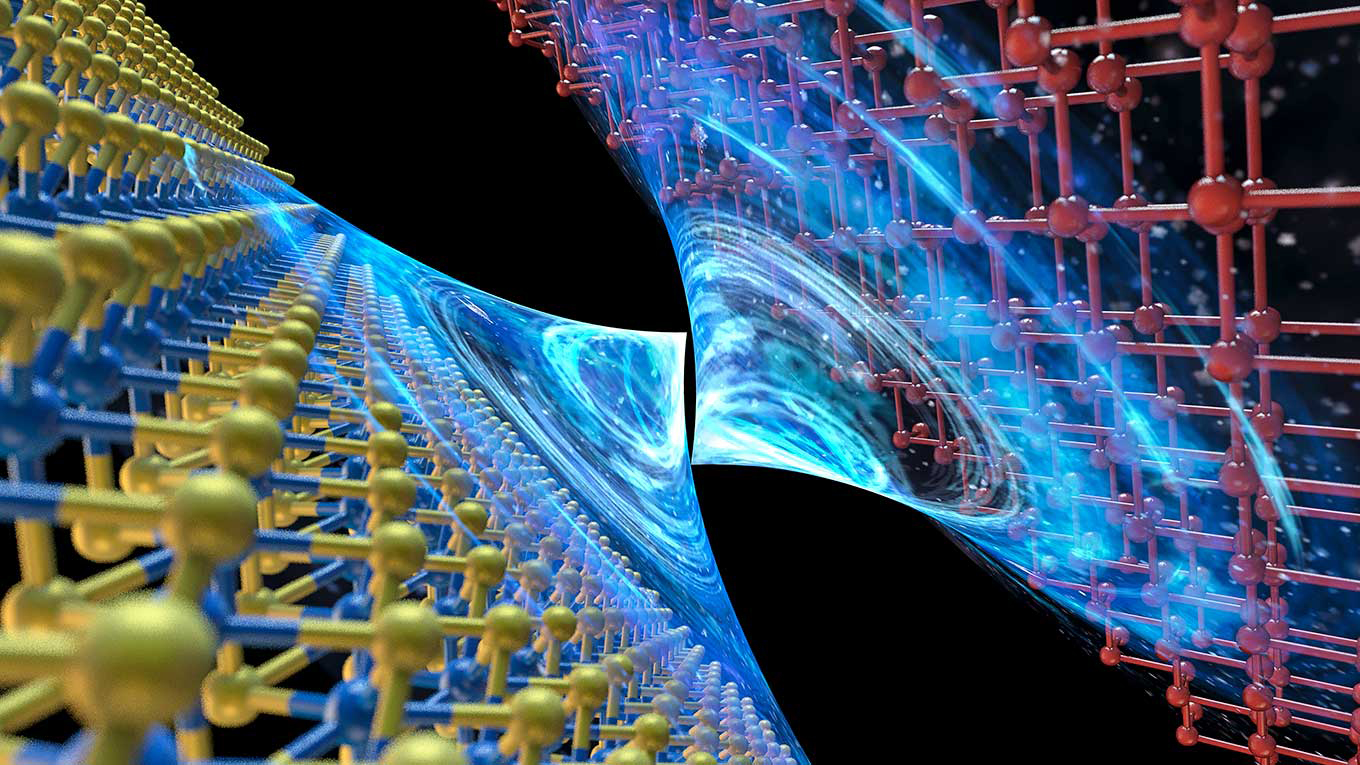
 At the interface between the semimetal (bismuth) and the 2D semiconductor (MoS2), there is no energy barrier for the electron to go through, leading to an ultralow contact resistance between them. (Image courtesy of the researchers.)
2D transistor technology overcomes barrier to ever-shrinking computer chips
A new advance led by researchers at MIT, UC Berkeley and the Taiwan Semiconductor Manufacturing Company makes it viable to replace bulky silicon-based transistors with atomically thin 2D materials.
The achievement, described in the journal Nature, could accelerate the development of a new generation of powerful computer chips in ever smaller packages. The four co-lead authors of the study are Pin-Chun Shen, Cong Su, Yuxuan Lin and Ang-Sheng Chou. Su and Lin began this research while they were Ph.D. students at MIT and continued the work as UC Berkeley postdoctoral researchers in physics and in electrical engineering and computer sciences, respectively.
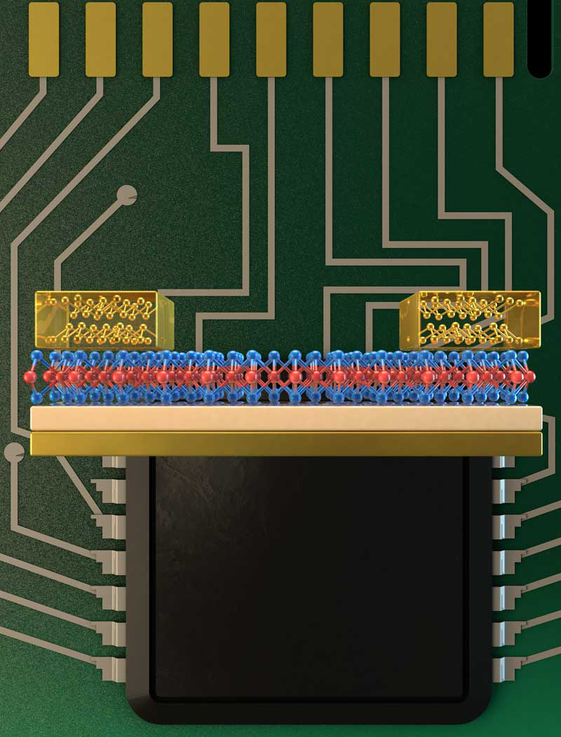
Researchers demonstrate extraordinary performance from miniaturized transistors, meeting the requirements for the technological roadmap for future transistors and microchips. (Image courtesy of the researchers.)
The researchers tackled the problem of the energy barrier that is universal between metals and semiconductors. This barrier, caused by the metal-induced gap state, prevents electrons from moving easily between the metal and semiconductor. In bulk semiconductors, this challenge is currently resolved through doping, but effective doping mechanisms are not available for 2D materials.
The researchers found the solution in using the element bismuth, a semimetal, to connect with molybdenum disulfide, an ultrathin monolayer. The properties of the semimetal combined with proper energy alignment between the two materials, led to fewer metal-induced gap states and eliminated the energy barrier.
“With this new technology, we solved a key bottleneck to creating 2D semiconductors,” said Lin, who is a postdoctoral researcher in the lab of Jeffrey Bokor, the Paul Gray Distinguished Professor of Engineering and chair of the Department of Electrical Engineering and Computer Sciences. “We can fabricate 2D transistors with a performance similar to state-of-the-art silicon technology, but with a much smaller footprint.”
Su now works in the lab of Alex Zettl, UC Berkeley professor of physics.
The work was supported by the National Science Foundation, the U.S. Army Research Office, the Office of Naval Research and the U.S. Department of Energy.
Learn more:
- Advance may enable ‘2D’ transistors for tinier microchip components (MIT news release)
- 2-D semiconductor contact resistances approach the quantum limit (UC Berkeley EECS news brief)
- Ultralow contact resistance between semimetal and monolayer semiconductors (Nature paper)