• Skip to primary navigation
  • Skip to main content
  • Departments
    • Aerospace Engineering
    • Bioengineering
    • Civil and Environmental Engineering
    • Electrical Engineering and Computer Sciences
    • Engineering Science
    • Industrial Engineering and Operations Research
    • Materials Science and Engineering
    • Mechanical Engineering
    • Nuclear Engineering
  • News
    • Berkeley Engineer magazine
    • Social media
    • News videos
    • News digest (email)
    • Press kit
  • Events
    • Commencement
    • Homecoming
    • Cal Day
    • View from the Top
    • Kuh Lecture Series
    • Minner Lecture
  • College directory
  • For staff & faculty
Berkeley Engineering

Educating leaders. Creating knowledge. Serving society.

  • About
    • Facts & figures
    • Rankings
    • Voices of Berkeley Engineering
    • Equity & inclusion
    • Leadership team
    • Milestones
    • Facilities
    • Maps
  • Admissions
    • Undergraduate admissions
    • Graduate admissions
    • Visit
    • Maps
    • Admissions events
    • K-12 outreach
  • Academics
    • Undergraduate programs
    • Majors & minors
    • Undergraduate Guide
    • Graduate programs
    • Graduate Guide
    • Innovation & entrepreneurship
    • Kresge Engineering Library
    • International programs
    • Executive education
  • Research & faculty
    • Centers & institutes
    • Undergrad research
    • Faculty
  • Students
    • Advising & counseling
    • Programs
    • Academic support
    • Student life
    • Wellness & inclusion
    • Undergraduate Guide
    • Degree requirements
    • Forms & petitions
    • Resources
  • Connect
    • Alumni
    • Industry
    • Give
    • Stay in touch
Home > News > Making monolayers work
Photoluminescence of MoS2 monolayer: before (left) and after superacid treatment

Making monolayers work

May 1, 2016
This article appeared in Berkeley Engineer magazine, Spring 2016

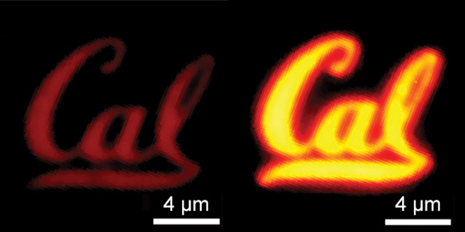
An emerging class of atomically thin materials known as monolayer semiconductors has generated a great deal of buzz in the world of materials science. Monolayers hold promise in the development of transparent LED displays, ultra-high efficiency solar cells, photo detectors and nanoscale transistors. Their downside? The films are notoriously riddled with defects, killing their performance. But Berkeley engineers have found a simple way to fix these defects by dipping molybdenum disulfine, or MoS2, into an organic superacid called bistriflimide, or TFSI. The treatment led to a dramatic 100-fold increase in the material’s photoluminescence quantum yield, a ratio describing the amount of light generated by the material versus the amount of energy put in — the greater the emission of light, the higher the quantum yield and the better the material quality. Their findings open the door to the practical application of monolayer materials in optoelectronic devices and high-performance transistors. Berkeley Engineering professors Ali Javey, Eli Yablonovitch and Xiang Zhang worked on the study with Ph.D. student Matin Amani, visiting Ph.D. student Der-Hsien Lien and postdoctoral fellow Daisuke Kiriya, as well as researchers from National Taiwan University, the University of Texas at Dallas and the U.S. Army Research Laboratory in Maryland.

Read more: Coming to a monitor near you: a defect-free, molecule-thick film

Topics: Materials science, Mechanical engineering
  • Contact
  • Give
  • Privacy
  • UC Berkeley
  • Accessibility
  • Nondiscrimination
  • instagram
  • twitter
  • linkedin
  • facebook
  • youtube
© 2022 UC Regents