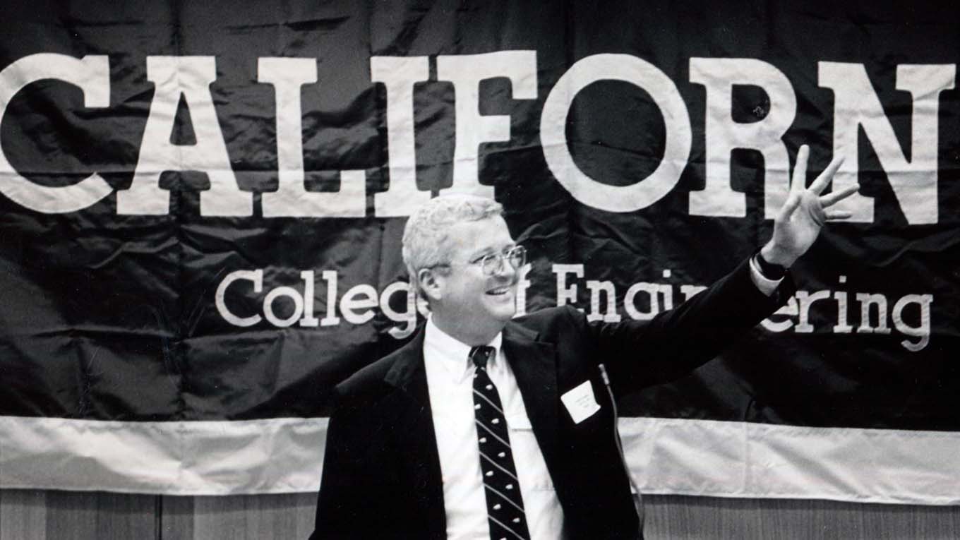
 David Hodges speaking at a 1992 Sproul Association Luncheon while he was dean of engineering. (Photo by Peg Skorpinski)
David Hodges, former dean of engineering and pioneer in integrated circuit design, dies at 85
David A. Hodges, a former dean of UC Berkeley’s College of Engineering whose pioneering work in integrated circuit design and semiconductor manufacturing helped ensure the continuation of Moore’s Law and contributed to the rapid growth of the tech industry, has died. He was 85.
Celebrate the life of David Hodges
Saturday, Feb. 18, 2023
1 p.m.
Faculty Club, UC Berkeley
Hodges was surrounded by family when he died at his Berkeley home on Sunday, Nov. 13, less than 18 months after he was diagnosed with ampullary cancer.
Over his nearly three-decade career at UC Berkeley, Hodges helped solidify the university’s reputation as the leading institution for research and education in integrated circuit (IC) design. He co-authored the textbook “Analysis and Design of Digital Integrated Circuits,” a classic used to teach digital IC design at universities around the world.
Even after he retired in 1998, he remained connected to the university and influential in the field of microelectronics, serving on various boards and committees in industry and at the Institute of Electrical and Electronics Engineers (IEEE).
‘A quiet changemaker’
“Dave Hodges was a gifted leader, at once visionary and practical, as well as a wise and compassionate man,” said Berkeley Chancellor Carol Christ. “He has been a trusted advisor to me during my chancellorship; he will be much missed.”
In 1990, Hodges became dean of the College of Engineering, a position he would hold for six years. During that time, Hodges established a development team for the college to better manage external relations and support growth in strategic directions. During his tenure, Hodges completed the fundraising for Soda Hall begun by his predecessor, Karl Pister, and he laid the early groundwork for a new Department of Bioengineering, which debuted in 1998.
“His foresight enabled the college not only to weather financial challenges at that time, but in subsequent years to more effectively raise funding for major programs and capital projects,” said Tsu-Jae King Liu, dean of the College of Engineering.
Paul Gray, former executive vice chancellor and provost and one of Hodges’ closest research collaborators, called Hodges “a quiet changemaker who was extraordinarily impactful in his various leadership roles.” Gray, who succeeded Hodges as dean of engineering, added that Hodges helped recruit him to UC Berkeley.
“People don’t often realize the influence he had because he preferred to remain behind the scenes,” said Gray. “He was always exceedingly generous in sharing credit for his many accomplishments.”
Engineering talent at an early age
Hodges was born in Hackensack, New Jersey, on Aug. 25, 1937, followed by two younger sisters. His parents were both graduates of Cornell University, and his father was an electrical engineer. According to family lore, Hodges managed to stick his father’s car keys into a wall socket and weld them together, emerging unscathed. “That’s when his parents knew he’d grow up to be an engineer,” said his daughter, Jennifer Hodges.
Growing up, Hodges continued his interest in electronics, earning a reputation — and a bit of pocket money — as someone who could reliably fix neighbors’ televisions and radios. Not surprisingly, he went on to study electrical engineering at Cornell University. Family members say that Hodges learned the value of collaboration and teamwork while staying at the Telluride House, a highly selective residential community at Cornell. Hodges earned his bachelor’s degree in electrical engineering at Cornell in 1960.
Hodges moved across the country for his graduate studies in electrical engineering at UC Berkeley, earning his M.S. degree in 1961 and his Ph.D. degree in 1966. It was during his Ph.D. studies that he met Susan Spongberg, a UC Berkeley graduate student in history who would occasionally help illustrate his papers with drawings of circuits. They wed in 1965 and had two children, Jennifer and Alan, in 1968 and 1974, respectively.
After graduating from UC Berkeley, Hodges returned to New Jersey to work at Bell Telephone Laboratories, conducting research and development for integrated circuits for communications. While at Bell Labs, Hodges saw the potential of metal-oxide-semiconductor (MOS) technology to shape the future of integrated circuits. Compared with bipolar junction transistors, which were predominant at that time, MOS transistors are easier to scale to smaller dimensions and consume less power, making them more amenable to very large-scale integration (VLSI) on a silicon chip. The pivot to MOS technology ensured the continuation of Moore’s Law, Gordon Moore’s observation that the number of transistors incorporated into the leading microprocessor chip doubles every two years.
Helping digital circuits make sense of an analog world
The challenge with MOS transistors, however, was that they were not well-suited to processing analog signals from the external world, such as light, sound and motion. When today’s mobile devices take photos, transmit our voices, sense their orientation and more, they are relying on the electronic chips inside them to translate analog signals to digital form for more efficient processing.

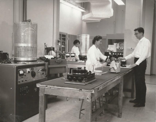
This 1963 image shows David Hodges (right) and Marina Bujatti (left), both engineering graduate students at the time, working with technician Dorothy McDaniel (center) in the Integrated Circuits Lab, a precursor to the Microlab at UC Berkeley.
Hodges first worked on combining analog and digital signal processing circuits on a single chip at Bell Labs for processing voice signals, leading to major advancements in digital telephony. He continued this line of research when he returned to UC Berkeley in 1970 as a faculty member. He teamed up with fellow engineering faculty members Paul Gray and Robert Brodersen to develop MOS analog-to-digital converters.
Hodges helped expand the applicability of the now-pervasive MOS technology to a wide range of applications in communications, signal processing and environmental sensing, among others, helping drive the rapid growth of the semiconductor industry and Silicon Valley.
Hodges was also the driving force behind the Berkeley Microfabrication Facility, or Microlab. It would replace the successful Integrated Circuit (IC) Laboratory, the world’s first university IC fabrication facility when it was established in 1962 by Hodges’ Ph.D. adviser, Don Pederson, and colleagues. Hodges lined up key support from campus faculty and leadership for the new Microlab, which would become a critical asset for microfabrication research across numerous departments. (The Microlab was succeeded by the Marvell Nanofabrication Laboratory in 2010.)
Around this time, Hodges shifted his focus to the problems he saw in domestic semiconductor manufacturing. He raised funds from the Sloan Foundation and industry partners to study the issue and, working with Robert Leachman, UC Berkeley professor of industrial engineering and operations research, to identify pain points to address.
Much of that research influenced the National Technology Roadmap for Semiconductors published by SEMATECH, a government-funded consortium designed to alleviate bottlenecks hindering semiconductor manufacturing in the United States.
“Building on his Microlab experience, Dave launched an entirely new research program in semiconductor manufacturing,” said Dean Liu. “Decades before the recent passage of the CHIPS and Science Act, Hodges understood early on how important semiconductor manufacturing would be for this country.”
A mentor to many
As impactful as his research achievements were, colleagues and former students consistently pointed to Hodges’ commitment as an educator. The large community of students he educated — including 27 who earned their doctoral degrees under his supervision — have gone on to influential positions around the world.

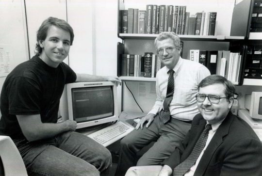
David Hodges (center) pictured here in 1990 with fellow faculty member Lawrence Rowe (right) and graduate student Brian Smith (left), working on the design of a new generation of CIM systems for semiconductor manufacturing. Visible on the terminal screen is the FMtool program, used for management of ultra-clean microelectronics fabrication equipment and facilities. (Photo by Peg Skorpinski)
“I never worked harder in my life than during my Ph.D., not because Dave pushed me, but because of his enthusiasm, which was contagious,” said Hae-Seung (Harry) Lee, who graduated from UC Berkeley in 1984 with a Ph.D. in electrical engineering and computer sciences. “When I first came up with the idea of self-calibration for my doctoral research, everybody was skeptical except Dave. He was more excited than I was. And when I hit rough patches, he never failed to encourage me, even through the most difficult times.”
Lee is now the Advanced Television and Signal Processing Professor of Electrical Engineering at the Massachusetts Institute of Technology. “I owe a big part of what I am today to Dave, and I dearly miss him,” he said.
“I like to make the distinction between those who are great teachers and those who are great educators,” said David Allstot, a professor of electrical and computer engineering at Oregon State University, who credits Hodges for recruiting him to UC Berkeley for his doctoral studies when he was an engineer at Tektronix. “Great teachers effectively pass on knowledge and skills to their students, but great educators go a step beyond to really inspire people. Dave was really good at that. He was a great educator.”
Allstot, who helped establish the David A. Hodges Endowed Fellowship with his wife, Vickie Allstot, added that it was a particularly exciting time to be studying integrated circuits. “Berkeley EECS was a locus of brilliant minds pushing boundaries to shape the future, and the faculty were all truly engaged with the students,” he said. “They helped usher in the shift from analog to digital telephony and a new era in microelectronics design.”
Leadership in academia and beyond
Hodges’ outstanding contributions in research and education have been recognized with numerous awards and honors, including his election to the National Academy of Engineering in 1983.
He held multiple leadership roles in IEEE and in 1978, was largely responsible for moving the International Solid-State Circuits Conference from Philadelphia to San Francisco. He was elected a Fellow of the IEEE and awarded the IEEE Education Medal. He also served as IEEE’s vice president of Publications, chair of the IEEE Awards Board, the founding editor of IEEE Transactions on Semiconductor Manufacturing, and editor of the IEEE Journal of Solid-State Circuits.
In 2013, Hodges was inducted into the Silicon Valley Engineering Hall of Fame.
Hodges is survived by his wife, Susan Hodges, and son, Alan Hodges, both of Berkeley; his daughter, Jennifer Hodges of Los Angeles; his sisters Caroline Persell of Sleepy Hollow, New York, and Nancy Walbek of Woods Hole, Massachusetts; and two granddaughters.
The family requests that memorial gifts be made to the David A. Hodges Fellowship and sent to UC Berkeley, Donor and Gift Services, 1995 University Avenue, Suite 400, Attn: Hodges Fellowship FW3107000, Berkeley, CA 94704-1070. Please note on your check that the gift is in memory of Dave Hodges.
A public memorial service for Hodges is being planned for early 2023. Information will be posted on the College of Engineering’s website when available.
