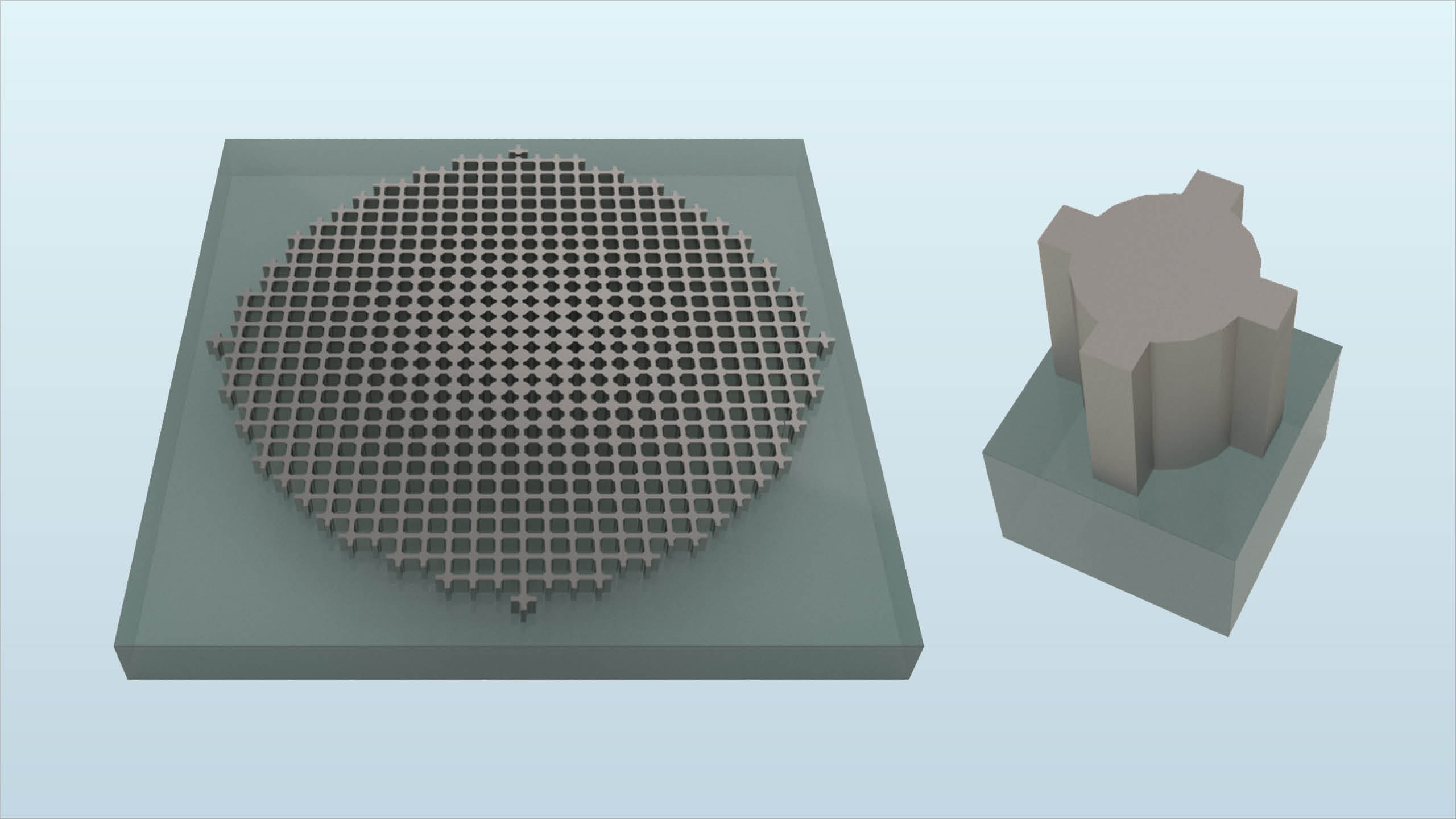
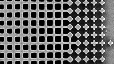
 Schematic of the fishnet metalens and a closeup (R) of its unit cell. The metalens is made of titanium dioxide. (Kante Lab image)
Engineers create game-changing metalens that breaks records in performance
Researchers at UC Berkeley have created an ultrathin, flat optical lens whose performance can finally rival that of bulkier, traditional lenses on the market. The development could lead to game-changing advances in solar energy, virtual reality technology, medical imaging and other applications reliant upon optics.
The researchers described their new metalens in a paper published today in Nature Communications. The lens measures 350-nanometers thick with an efficiency of 70% over a frequency spanning visible to infrared light.

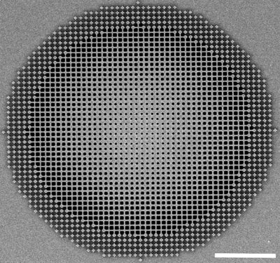
Shown is the fishnet achromatic metalens developed by Berkeley engineers. The scale bar is 5 micrometers. (Jeongho Ha image)
“This is the first photonic system with such a broad bandwidth and such high efficiencies in an ultrathin flat lens,” said study principal investigator Boubacar Kanté, associate professor of electrical engineering and computer sciences and faculty scientist at Lawrence Berkeley National Laboratory. “This is, simply, the thinnest, most efficient, broadest band flat lens in the world.”
Lead authors of the study are graduate student Liyi Hsu and postdoctoral researcher Abdoulaye Ndao in Kanté’s lab.
The size and weight of optical lenses have presented significant obstacles in the effort to miniaturize optoelectronics and other devices. Traditional lenses, one of the most basic components in optics, are usually made with bulk materials and curved surfaces to bend and focus incoming light waves. Such lenses are able to capture 65–75% of the incident light, but they are relatively heavy and susceptible to chromatic aberrations, the distortions that result due to the dependence of the refractive index on the color of light.
Flat lenses use engineered designs and characteristics of different metamaterials to bend light. They are appealing to researchers because such metalenses are capable of manipulating light at subwavelength scales, and they can overcome chromatic aberrations, but only in a very narrow band of light. Until now.
Going flat has often meant sacrificing performance in lenses. Previous metalenses delivered lower efficiencies of 20–40% in lenses measuring 600–800 nanometers thick. A sheet of paper, in comparison, is about 100,000 nanometers thick.
The researchers came up with an innovative solution to improve the light-capturing capabilities of their flat metalens. They used electron-beam lithography to shape a fishnet pattern onto a titanium dioxide wafer. To mimic the curvature of a traditional lens, they used a gradient in which smaller holes were formed in the center and larger ones were positioned around the edges.
They demonstrated the ability of their fishnet-achromatic metalens to capture 70% of incoming light in frequencies ranging from 640 nanometers (reddish-orange light) to 1200 nanometers (infrared light). Light entering the fishnet metalens within that broad octave band of wavelengths would be focused at a single point on the other side of the lens.
“We are very excited by these results because many applications required the simultaneous processing of multiple wavelengths in a broad spectrum,” said Kanté. “This is the case for solar energy applications where we need to focus all color of light for efficient solar cells or solar concentrators.”
The lighter-weight metalens also reduces the power consumption for a variety of applications, said Kanté. As an example, satellites, where every ounce counts, would require less fuel to launch and operate if metalenses replaced traditional ones.
A good next step, Kanté said, would be to develop processes that could scale up for larger scale production.
Other study co-authors are Connie Chang-Hasnain, Jeongho Ha and Jun-Hee Park from the Department of Electrical Engineering and Computer Sciences.
This research was primarily supported by the Department of Energy. Additional funding was provided by the National Science Foundation, the Office of Naval Research and the Defense Advanced Research Projects Agency.

