Moving data at the speed of light

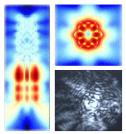
LIGHTING THE WAY: The unique structure of the nanopillars grown by researchers strongly confines light in a tiny volume to enable subwavelength nanopillars. Images on the left and top right show simulated electric field intensities that describe how light circulates helically inside the nanopillars. On the bottom right is an experimental camera image of laser light from a single nanolaser. (Photo by Connie Chang-Hasnain Group.)
Modern computing has a looming traffic problem.
No, not the jam of cars along the highways of Silicon Valley — but a serious data traffic problem.
Every two years, the computer hardware industry has doubled the number of transistors that can be placed inexpensively on an integrated circuit. This historical trend, known as Moore’s Law, has become the standard in the semiconductor industry for planning, research and development, allowing for higher system performance and the continual improvement of data speeds.
At least until now.
Sometime in the next decade, experts say, processors will not be able to deliver better performance, because integrated circuits will have reached their capacity. Commonly described as interconnect bottleneck, this phenomenon means that computers, regardless of their processing speed, will be incapable of moving data any faster.
But Berkeley engineers have recently developed a groundbreaking process that could solve the vexing problem of interconnect bottleneck and lead to a new class of faster, more efficient microprocessors.
The research team, led by Connie Chang-Hasnain, professor of electrical engineering and computer sciences (EECS), has found an innovative way to grow nanolasers directly onto a silicon surface and take advantage of the superior data carrying capacity of light particles.
Optoelectronic chips have long been touted as a solution to overcoming the interconnect bottleneck. Light particles have the inherent ability to carry far more data than electrical signals, but silicon, the material that forms the foundation of modern electronics, is extremely deficient at generating light. So engineers have looked to another class of materials known as III-V (“three-five”) semiconductors to create light-based components such as light-emitting diodes (LEDs) and lasers.
But marrying III-V semiconductors with silicon to create a single optoelectronic chip has been problematic. For one, the atomic structures of the two materials are mismatched.
“Growing III-V semiconductor films on silicon is like forcing two incongruent puzzle pieces together,” says study lead author Roger Chen, a graduate student in EECS working under the guidance of Chang-Hasnain. “It can be done, but the material gets damaged in the process.”

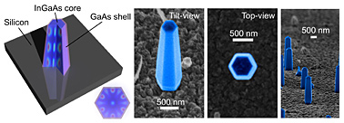
IN THE CHIPS: A schematic (left) and various scanning electron microscope images of nanolasers grown directly on a silicon surface. This achievement by Berkeley researchers could lead to a new class of optoelectronic chips.(Photo by Connie Chang-Hasnain Group.)
Moreover, the semiconductor manufacturing industry is set up for the production of silicon-based materials, so for practical reasons, the goal has been to integrate the fabrication of III-V devices into standard chip manufacture.
“Today’s massive silicon electronics infrastructure is extremely difficult to change for both economic and technological reasons, so compatibility with silicon fabrication is critical,” says Chang-Hasnain. “One problem [with this] is that growth of III-V semiconductors has traditionally involved high temperatures — 700 degrees Celsius or more — that would destroy the electronics. Meanwhile, other integration approaches have not been scalable.”
The researchers overcame this limitation by finding a way to grow nanopillars made of indium gallium arsenide, a III-V material, onto a silicon surface at the relatively cool temperature of 400 degrees Celsius.
The researchers used metal-organic chemical vapor deposition to grow the nanopillars on the silicon. Once the nanopillar was made, the researchers showed that it could generate near infrared laser light — a wavelength of about 950 nanometers — at room temperature. The tapered, hexagonal structure of the nanopillars creates a new, efficient, light-trapping optical cavity. Light circulates up and down the structure in a helical fashion and amplifies via this optical feedback mechanism.
The unique approach of growing nanolasers directly onto silicon could lead to highly efficient silicon photonics. The researchers noted that the miniscule dimensions of the nanopillars — smaller than one wavelength on each side, in some cases — make it possible to pack them into small spaces with the added benefit of using very little energy.
“Ultimately, this technique may provide a powerful and new avenue for engineering on-chip nanophotonic devices such as lasers, photodetectors, modulators and solar cells,” says Chen.
The team’s groundbreaking research, described in the cover story of the March 2011 issue of Nature Photonics, “has the potential to catalyze an optoelectronics revolution in computing, communications, displays and optical signal processing,” says Chang-Hasnain.
